- AMD Community
- Support Forums
- General Discussions
- Re: 12 nm or 14 nm?!
General Discussions
- Subscribe to RSS Feed
- Mark Topic as New
- Mark Topic as Read
- Float this Topic for Current User
- Bookmark
- Subscribe
- Mute
- Printer Friendly Page
- Mark as New
- Bookmark
- Subscribe
- Mute
- Subscribe to RSS Feed
- Permalink
- Report Inappropriate Content
12 nm or 14 nm?!

This is Max. I want to supplement my request about the false information that is distributed on the Internet of Russia, about your second generation processors. I found another well-known video ( https://youtu.be/WCiOgbOhPpA?t=568 ) and here it is translated into Russian as - there is no difference in the physical sizes of the transistors used in the generation of Ryzen 2 !
That is, the person says that your new processors are no different from the old first-generation 14-nanometer! Accordingly, I read reviews in electronics supermarkets ( https://www.dns-shop.ru/product/06bf9e32275d3330/processor-amd-ryzen-5-2600-box/opinion/ ) are now users of each other discourage buying processors amd, as they say your 12-meters is just marketing and not reality. Take action! Waiting for an answer.
- Mark as New
- Bookmark
- Subscribe
- Mute
- Subscribe to RSS Feed
- Permalink
- Report Inappropriate Content
I think there is a measure of confusion, at least for Consumers when it comes to Process Nodes below 32nm.
Those being 28nm, 22nm, 18nm, 16nm, 14nm, 12nm, 10nm and 7nm.
Now, I'm not going to delve too deeply down the rabbit hole of a Process Node Specification and how few actually are in line with them. What I will do instead is simplify this to make it easier to understand what's going on from a more laymen perspective.
So a good way to look at Process Nodes is in two key elements.
The Node Grid and the Element (Transistor) Size.
Now typically speaking these should both be the same.
This means that we would have, say 32nm Elements on a 32nm Grid.
Yet when we move to "28nm" ... this is no longer true.
We are instead talking about 28nm Elements but we are still on a 32nm Grid.
Should we take the FX 4300 and X4 830K as examples of these, then physically these Processors take the same amount of Silicon Space, have the exact same Layout, etc.
What's different is that the X4 830K is using 28nm Elements... the result of which is that instead of being that instead of using 125w, it is only using 95w of Power. It also produces ~3.8% Less Heat / Watt, because you have said unused Silicon that dissipates the excess heat better... so even if you were to Down-Clock the FX 4300 to use only 95w, then you would still see a Lower Temperature produced from the X4 830K.
Assuming we're using the same 125w TDP Cooler (such as the Wraith Cooler), well this means instead of 58c Avg. Temperature (assuming a 21c Ambient); then we'd be looking instead at 55c Avg.
This as a note means we can push said Processors much further in terms of Frequencies, not just seeing Lower Temperatures, Lower Power Consumption but also as there is more room between Transistors., it also means we have more Logic Stability at Higher Frequencies where the Voltage has a habit of "Leaking" through and triggering Neighbouring Transistors.
For those curious, this is generally known as "Quantum Tunneling" and was a major issue in the effort to produce a 14nm Process Node. Don't worry, I won't delve into this aspect too deeply... but the general premise of it is that when you get down to a small enough node there's a concept that the Voltage will "Teleport" through the Walls between the Circuitry and that it only exists at said smaller Nodes.
This isn't accurate to what the phenomenon is, but as it's not strictly important to what we're discussing I'll skip a proper explanation for now... just know that there was an issue with Densely Packed Low-Voltage Triggered Transistors that the smaller we go, the less effective the "Walls" between said Transistors become to prevent the Voltage from simply passing through and triggering something it isn't supposed to.
So, how do we resolve this?
Well ... this was (mostly) resolved through Fin FET Technology., which is basically a fancy way of saying that each Transistor Wall isn't a Singular Wall but instead is 2 - 4 Walls that with each of these "Fins" there is a reduction in enough Voltage getting through to Trigger the Low-Voltage Transistors.
Of course, this then results in a problem... as for example a 14nm Transistor, now requires another 1-2nm of "Insulation".
As such; while you can have 14nm Transistors, you need to essentially be on a larger Node Grid.
Say 22/18/16nm, so that you can space out the Transistors enough to account for the Insulation.
So, now comes the question.
If you're using a 16nm Grid but 14nm Transistors... well what is it? 16nm or 14nm?
This is where the subjective element comes into play.
Let's take Intel's Ivy Bridge as a good example here. As it is a 25nm Node Grid but 22nm Transistors.
Intel, of course, marketed it as a 22nm Node... but strictly speaking, it's 25nm.
This trend would continue as Haswell was 22/20nm, Broadwell was 18/14nm, Skylake was 16/14nm and Coffee Lake is 15/14nm.
I'd imagine that Cascade Lake is actually 12/10nm., although Intel has been having serious issues with it.
When we switch over to AMD,. well, things get a little "Complicated" ...
So Zen is 14nm,. as what Global Foundries / Samsung did was they optimised the High/Low Trigger for their Transistors... hence why Zen / Polaris doesn't have a "Soft" Instability Limit., but rather when it hits the ASIC Quality Limit; it like flipping a switch from "It Works" to "It Does't Work" ... typically speaking you'll have a "Soft" area, where you'll have increasing issues from randomly triggered Transistors from just normal quality variance; where-as with Zen / Polaris, that's simply not the case. You'll trigger MOST of them causing a complete Logic Lock that requires the Processor to be Reset.
On top of this, they kept the Frequency Clocks ~15% Below their Quality Specification Threshold.
It gets a little messy getting into "Overclocking" and "Underclocking" regarding Processors today., but arguably speaking this is an 'Underclock' from where the Architecture was designed/intended to Clock at.
So we can in this instance say that both the Transistors were altered to have a Higher Trigger Tolerance, with Underclocking to reduce the Voltage peak.
I guess this isn't too important as to the Grid/Element Node Process but might be interesting for those curious about how AMD/Samsung/GloFo were capable of getting a "True" 14nm Process.
Still, keep in mind it isn't actually operating as a 14nm Process should. That is to say, that it isn't really quite as efficient and this is why NVIDIA/TSMC' 16/14nm was (at launch) a more efficient approach., at the cost of slightly more silicon space.
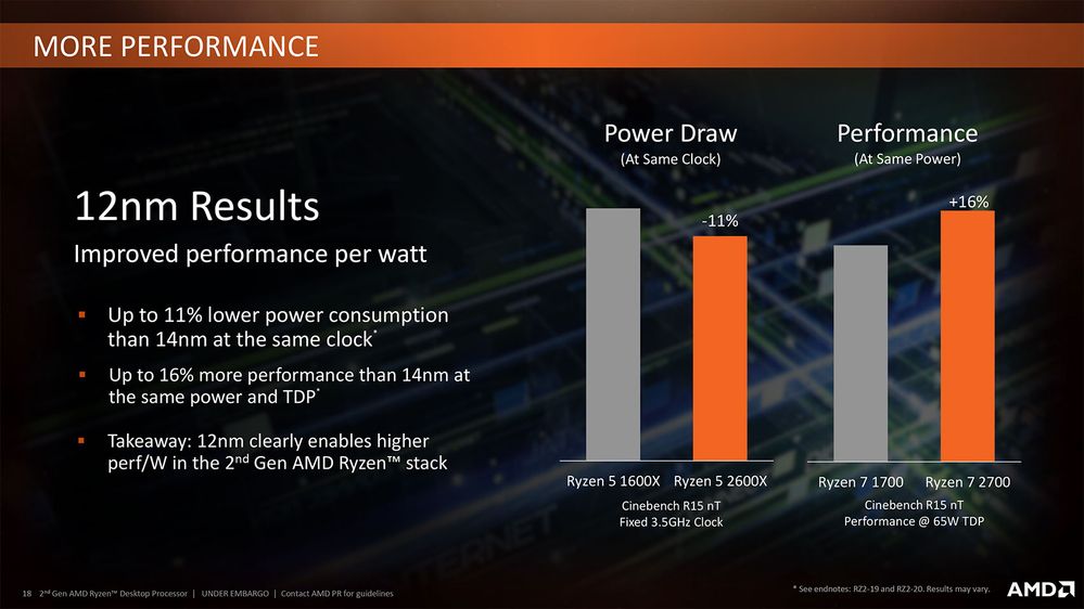
As we now look at Zen+ and Polaris 30... both of these are 14/12nm., so physically speaking they're using an identical space to their previous 14nm versions., but using smaller Transistors actually puts them in line with the Theoretical 'Ideal' 14nm improvements that should've been seen.
That is to say that 14/12nm = 14nm Efficiency as opposed to 14nm = 16-15nm Efficiency.
Both as noted at taking up the same space., it's just one is much more efficient; capable of Higher Clocks while using far less Power.
Hopefully this clears it up a bit.
- Mark as New
- Bookmark
- Subscribe
- Mute
- Subscribe to RSS Feed
- Permalink
- Report Inappropriate Content
I understood this small transistor (12nm) on large tracks (14nm). Thank.
True, the video said that the physical size of the transistor has not changed (
