- AMD Community
- Communities
- Developers
- Server Processors
- Understanding Zen3+ UMC channels
Server Processors
- Subscribe to RSS Feed
- Mark Topic as New
- Mark Topic as Read
- Float this Topic for Current User
- Bookmark
- Subscribe
- Mute
- Printer Friendly Page
- Mark as New
- Bookmark
- Subscribe
- Mute
- Subscribe to RSS Feed
- Permalink
- Report Inappropriate Content
Understanding Zen3+ UMC channels
Hello,
( I hope this is the right forum for the issue )
According to AMD specs "Processor Programming Reference (PPR) for AMD Family 19h Model 11h, Revision B1 Processors", bit 31 "SdpInit" of "SDP Control" register has to be set for each enabled UMC channel. Address 0xN50104 where N is the channel number to probe.

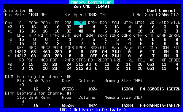
I can guarantee this algorithm is perfectly working on all Zen1 up to Zen4 where for instance only two "SDP Control" have bit 31 set on a Dual Channel setup. As a reference, below, Zen2/Matisse where SDP is correctly decoded.
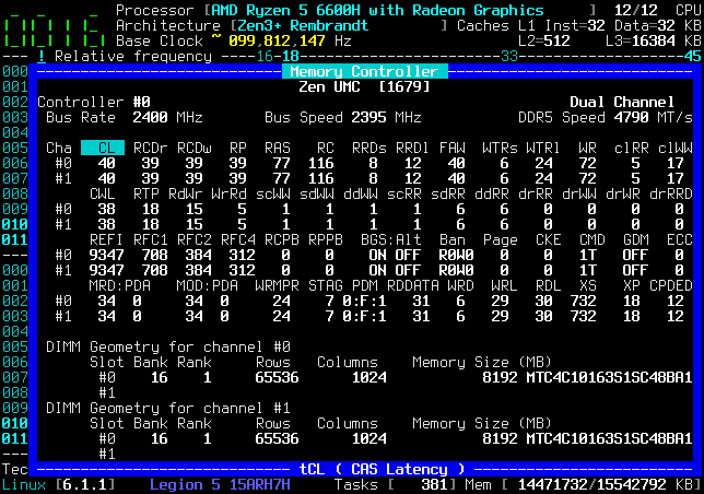
Now my problematic case with Rembrandt Ryzen 5 6600H
Ryzen 5 6600H is here configured with two 8GB DIMM ref "MTC4C10163S1SC48BA1", thus I'm expecting to read a pair of SDP Control as enabled but not all four registers 0x050104, 0x150104, 0x250104, 0x350104 bit 31 set.
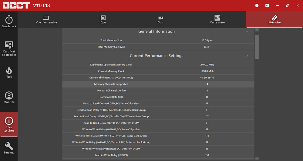
- Windows OCCT
- Linux CoreFreq
 Cha   CL  RCDr RCDw  RP  RAS   RC  RRDs RRDl FAW  WTRs WTRl  WR  clRR clWW
  #0   40   39   39   39   77  116    8   12   41    6   25   73    5   18
  #1   40   39   39   39   77  116    8   12   41    6   25   73    5   18
  #2   40   39   39   39   77  116    8   12   41    6   25   73    5   18
  #3   40   39   39   39   77  116    8   12   41    6   25   73    5   18
      CWL  RTP RdWr WrRd scWW sdWW ddWW scRR sdRR ddRR drRR drWW drWR drRRD
  #0   38   18   15    5    1    2    2    1    6    6    0    0    0    0
  #1   38   18   15    5    1    2    2    1    6    6    0    0    0    0
  #2   38   18   16    5    1    2    2    1    6    6    0    0    0    0
  #3   38   18   16    5    1    2    2    1    6    6    0    0    0    0
      REFI RFC1 RFC2 RFC4 RCPB RPPB  BGS:Alt  Ban  Page  CKE  CMD  GDM  ECC
  #0  9375  710   32    6   0    0    ON OFF  R0W0   0    0   1T    ON   0
  #1  9375  710   32    6   0    0    ON OFF  R0W0   0    0   1T    ON   0
  #2  9375  710   32    6   0    0    ON OFF  R0W0   0    0   1T    ON   0
  #3  9375  710   32    6   0    0    ON OFF  R0W0   0    0   1T    ON   0
      MRD:PDA   MOD:PDA  WRMPR STAG PDM RDDATA WRD  WRL  RDL  XS   XP CPDED
  #0   34  0     34  0     24    7 0:F:1   31   6   29   30  735   18   12
  #1   34  0     34  0     24    7 0:F:1   31   6   29   28  735   18   12
  #2   34  0     34  0     24    7 0:F:1   31   6   29   30  735   18   12
  #3   34  0     34  0     24    7 0:F:1   31   6   29   30  735   18   12

 DIMM Geometry for channel #0
      Slot Bank Rank     Rows   Columns    Memory Size (MB)
       #0    16    1     65536      1024           8192 MTC4C10163S1SC48BA1
       #1
 DIMM Geometry for channel #1
      Slot Bank Rank     Rows   Columns    Memory Size (MB)
       #0    16    1     65536      1024           8192 MTC4C10163S1SC48BA1
       #1
 DIMM Geometry for channel #2
      Slot Bank Rank     Rows   Columns    Memory Size (MB)
       #0    16    1     65536      1024           8192 MTC4C10163S1SC48BA1
       #1
 DIMM Geometry for channel #3
      Slot Bank Rank     Rows   Columns    Memory Size (MB)
       #0    16    1     65536      1024           8192 MTC4C10163S1SC48BA1
       #1
As you can see in screenshot, the Memory Channels Supported but especially Active is four.
4 supported is architecturally correct to my understanding of Rembrandt. although I'm still wondering how 4 channels can be activated with two DIMM installed ? And the consequences on the SDP registers.
Not talking about SPD, SMBIOS, DMI or other instrumentation, how I'm suppose to decode the number of active channels from the UMC registers (via SMU) ?
It is probably the way the architecture is designed for Rembrandt but that's the only case I have encountered so far. For instance, Raphael UMC decoding on 7950X is this time decoded as two channels for a DDR5 platform.
I'm ready to change my code to a new DDR5 decoding algorithm to work with both Zen3+ and Zen4 but I would like to understand what's new in the registers.
Cyril
Solved! Go to Solution.
- Mark as New
- Bookmark
- Subscribe
- Mute
- Subscribe to RSS Feed
- Permalink
- Report Inappropriate Content
Issue is finding a solution.
- Mark as New
- Bookmark
- Subscribe
- Mute
- Subscribe to RSS Feed
- Permalink
- Report Inappropriate Content
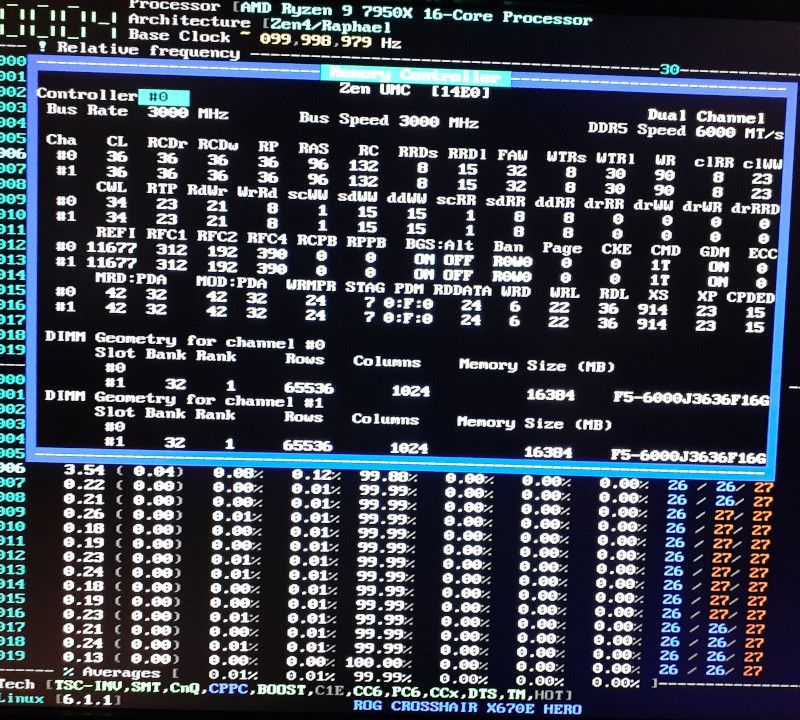
Progress to decode UMC with DDR5 has been made for Raphael
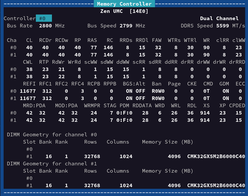
For Rembrandt, CoreFreq will now apply two sub-channels:
- Mark as New
- Bookmark
- Subscribe
- Mute
- Subscribe to RSS Feed
- Permalink
- Report Inappropriate Content
8 Unified Memory Controller (UMC)
8.1 DDR5 Overview
Each processor IOD includes twelve Unified Memory Controllers (UMC). Each UMC controls two DDR5 32-bit channels routed to the same DDR5 DIMM.
- Mark as New
- Bookmark
- Subscribe
- Mute
- Subscribe to RSS Feed
- Permalink
- Report Inappropriate Content
DDR5 Quad Channel with 2 DIMMs?
White Paper Migration to DDR5 Memory Modules
Two installed DIMMs
Rembrandt
Sum of all SDP = 4
Raphael
Sum of all SDP = 2
- Mark as New
- Bookmark
- Subscribe
- Mute
- Subscribe to RSS Feed
- Permalink
- Report Inappropriate Content
Issue is finding a solution.
