- AMD Community
- Support Forums
- PC Processors
- Re: Do Ryzen support write-back caching for Memory...
PC Processors
- Subscribe to RSS Feed
- Mark Topic as New
- Mark Topic as Read
- Float this Topic for Current User
- Bookmark
- Subscribe
- Mute
- Printer Friendly Page
- Mark as New
- Bookmark
- Subscribe
- Mute
- Subscribe to RSS Feed
- Permalink
- Report Inappropriate Content
Do Ryzen support write-back caching for Memory Mapped IO (through PCIe interface)?
In kernel module, I set MTRR (Memory Type Range Register) and PTE (Page Table Entry) as write-back cache, referring to AMD System Programming manual. (https://developer.amd.com/wordpress/media/2012/10/24593_APM_v21.pdf)
But the write request is sent to FPGA as only word size (4byte).
Unlike write, the read request is sent to the FPGA with cache block size (64 bytes) as if it were a write-through cache.
So I wonder if it does not support write-back cache.
I would appreciate your advice.
Thank you.
Gyeong Il Min edits the message.
My system is follow:
- OS: Ubuntu 16.04
- CPU: Ryzen 7 1700
- Motherboard: ASRock X370 Taichi
- MMIO device: Xilinx Kintex7 Evaluation FPGA board (KC705)
- Mark as New
- Bookmark
- Subscribe
- Mute
- Subscribe to RSS Feed
- Permalink
- Report Inappropriate Content
gyeong9m, most of your terms I do not recognize, suggesting that you are running Linux. I cannot help with Linux but some here can but they will require some information. Please tell us your OS and HW specifications. Here are mine as an example:
ASRock Fatal1ty X399 Pro Gaming, Threadripper 1950X, 2xSamsung SSD 960 EVO RAID, 1TB &
500 GB WD Black, G.SKILL [Flare X (for AMD)] F4-3200C14Q-32GFX, Windows 10 x64 Pro,
Enermx Platimax 850, Enermx Liqtech TR4 CPU Cooler, Radeon RX580, BIOS 2.0
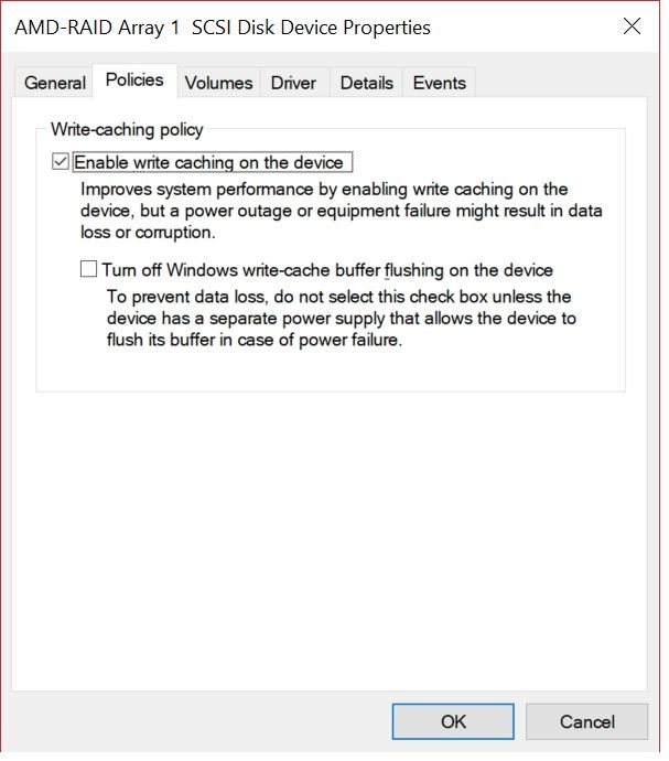
Here is the policy for my SSD RAID0 NVMe and therefore PCIe:
I have run with write-cache buffer flushing both enabled and disabled with very measurable results. This may not answer your question, but I suspect Linux people will need more information. Enjoy, John.
- Mark as New
- Bookmark
- Subscribe
- Mute
- Subscribe to RSS Feed
- Permalink
- Report Inappropriate Content
misterj, thank you for your quick reply.
However, I think that 'write cache' in your screenshot means cache inside SSD device.
I'm interested in the cache inside the processor.
If my opinion is wrong, I would appreciate it if you pointed it out.
Thank you.
(I will update my system environment information, following your advice.)
- Mark as New
- Bookmark
- Subscribe
- Mute
- Subscribe to RSS Feed
- Permalink
- Report Inappropriate Content
I think you are correct, gyeong9m. And sorry, I cannot answer your question. I would suggest you open an AMD Online Service Request. Good luck and enjoy, John.
EDIT: Since the 'write cache' in my screenshot is for a RAID0 (2 SSDs), the cache may be somewhere else. Found some documents that have lots of block diagrams that will mean much more to you. There are only three Family 17h documents and other users looking for these are not finding what they need (still under NDA). Please DL them and see if there is any help. I still believe opening a Support Ticket is the best way to go. link
- Mark as New
- Bookmark
- Subscribe
- Mute
- Subscribe to RSS Feed
- Permalink
- Report Inappropriate Content
Thank you for your kind advice.
I'll open an AMD Online Service Request.
Thank you.
- Mark as New
- Bookmark
- Subscribe
- Mute
- Subscribe to RSS Feed
- Permalink
- Report Inappropriate Content
I had a similar question and a solution.
However, the kernel must be recompiled.
- Mark as New
- Bookmark
- Subscribe
- Mute
- Subscribe to RSS Feed
- Permalink
- Report Inappropriate Content
I played with this a little and learned some. Using Windows Kit SDK (WinDbg) I was able to run a Local Kernel debug session on my 1950X and display MTRR:
MTRR: Var 8, Fixed-support enabled, USWC-supported, Default: UC
WB:00000-0ffff WB:10000-1ffff WB:20000-2ffff WB:30000-3ffff
WB:40000-4ffff WB:50000-5ffff WB:60000-6ffff WB:70000-7ffff
WB:80000-83fff WB:84000-87fff WB:88000-8bfff WB:8c000-8ffff
WB:90000-93fff WB:94000-97fff WB:98000-9bfff WB:9c000-9ffff
WT:a0000-a3fff WT:a4000-a7fff WT:a8000-abfff WT:ac000-affff
WT:b0000-b3fff WT:b4000-b7fff WT:b8000-bbfff WT:bc000-bffff
UC:c0000-c0fff UC:c1000-c1fff UC:c2000-c2fff UC:c3000-c3fff
UC:c4000-c4fff UC:c5000-c5fff UC:c6000-c6fff UC:c7000-c7fff
UC:c8000-c8fff UC:c9000-c9fff UC:ca000-cafff UC:cb000-cbfff
UC:cc000-ccfff UC:cd000-cdfff UC:ce000-cefff UC:cf000-cffff
UC:d0000-d0fff UC:d1000-d1fff UC:d2000-d2fff UC:d3000-d3fff
UC:d4000-d4fff UC:d5000-d5fff UC:d6000-d6fff UC:d7000-d7fff
UC:d8000-d8fff UC:d9000-d9fff UC:da000-dafff UC:db000-dbfff
UC:dc000-dcfff UC:dd000-ddfff UC:de000-defff UC:df000-dffff
WP:e0000-e0fff WP:e1000-e1fff WP:e2000-e2fff WP:e3000-e3fff
WP:e4000-e4fff WP:e5000-e5fff WP:e6000-e6fff WP:e7000-e7fff
WP:e8000-e8fff WP:e9000-e9fff WP:ea000-eafff WP:eb000-ebfff
WP:ec000-ecfff WP:ed000-edfff WP:ee000-eefff WP:ef000-effff
WP:f0000-f0fff WP:f1000-f1fff WP:f2000-f2fff WP:f3000-f3fff
WP:f4000-f4fff WP:f5000-f5fff WP:f6000-f6fff WP:f7000-f7fff
WP:f8000-f8fff WP:f9000-f9fff WP:fa000-fafff WP:fb000-fbfff
WP:fc000-fcfff WP:fd000-fdfff WP:fe000-fefff WP:ff000-fffff
Variable: Base Mask Length
0. WB: 00000000:00000000 0000ffff:80000000 00000000:80000000
1. WB: 00000000:80000000 0000ffff:c0000000 00000000:40000000
2. UC: 00000000:bc000000 0000ffff:fc000000 00000000:04000000
3.
4.
5.
6.
7.
Hopefully this will help a little. Enjoy, John.
- Mark as New
- Bookmark
- Subscribe
- Mute
- Subscribe to RSS Feed
- Permalink
- Report Inappropriate Content
Thank you for your response, tuxine, misterj.
The issue in your link is related for my issue.
But I think your issue is that linux does not automatically register the memory space(marked red in your link, 0x0000DF000000) to MTRR.
And after modifying kernel .config file, the linux kernel automatically resgister the memory space to MTRR. (If my opinion is wrong, I would appreciate it if you pointed it out.)
However, my problem is the processor does not work as MTRR configuration.
I have written a kernel module to configure MTRR for my target memory space and have verified that it works as follows (important parts are marked in red):
This is my target memory space:
$ lspci -v -s 0f:00
0f:00.0 Memory controller: Xilinx Corporation Device 7022
Subsystem: Xilinx Corporation Device 0007
Flags: fast devsel
Memory at 80000000 (64-bit, prefetchable)
This is MTRR state after executing my kernel code:
$ cat /proc/mtrr
reg00: base=0x000000000 ( 0MB), size= 2048MB, count=1: write-back
reg01: base=0x07f000000 ( 2032MB), size= 16MB, count=1: uncachable
reg02: base=0x080000000 ( 2048MB), size= 1024MB, count=0: write-back
After the MTRR is configured as write-back properly, it works for read request (the size of request is changed from 4-byte (word size) to 16-byte(cache block size)).
But write requset is still sent by word size as if its configuration is write-through.
Thank you.
(I opened an AMD Online Service Request and I'm still waiting for response.)
- Mark as New
- Bookmark
- Subscribe
- Mute
- Subscribe to RSS Feed
- Permalink
- Report Inappropriate Content
gyeong9m, I have been using your thread to learn a little about memory and paging. It seems to me that there is a potential conflict between Memory Type Range Register (MTTR) and Page Table Entry (PTE)/Page Attribute Table (PAT). I think there is little information on all this in Windows because there are no mechanisms (at least that I can find) to manage them. You did not show us the code you used to set your memory type, but I was wondering did you set the PTE/PAT to be compatible with MTRR? Who wins if there is a conflict? Can you post your MTRR before and after your code runs? Please let us hear what your learn from AMD. Thanks and enjoy, John.
- Mark as New
- Bookmark
- Subscribe
- Mute
- Subscribe to RSS Feed
- Permalink
- Report Inappropriate Content
Sorry for providing not enough information.
MTRR determines cache attribute for a physical memory space, and PTE/PAT determines cache attribute of a virtual memory space.
Cache attribute of a virtual memory space should be same with that of the physical memory space.
So we set both of MTRR and PTE/PAT by write-back cache as follow.
First, here is our physical address of target device and default MTRR state:
$ lspci -v -s 0f:00
0f:00.0 Memory controller: Xilinx Corporation Device 7022
Subsystem: Xilinx Corporation Device 0007
Flags: fast devsel
Memory at 80000000 (64-bit, prefetchable) [disabled] [size=1G]
$ cat /proc/mtrr
reg00: base=0x000000000 ( 0MB), size= 2048MB, count=1: write-back
reg01: base=0x07f000000 ( 2032MB), size= 16MB, count=1: uncachable
After running our kernel code, a new MTRR entry for our target device is inserted:
$ cat /proc/mtrr
reg00: base=0x000000000 ( 0MB), size= 2048MB, count=1: write-back
reg01: base=0x07f000000 ( 2032MB), size= 16MB, count=1: uncachable
reg02: base=0x080000000 ( 2048MB), size= 1024MB, count=0: write-back
Then, we allocate a virtual memory space to the target device and set PTE/PAT for the memory space.
Here is our kernel code:
int dummyKernelModule_init(void) { // main function of the kernel module
...
BAR_virt = pcim_iomap(pci_xilinx_dev, 0, len); // allocate virtual memory space for the target device
printk(KERN_INFO "dummyKernelModule : BAR_virt %p - %x\n", BAR_virt, len); // print address of the virtual memory space
dummyKernelModule_print_pte(BAR_virt); // print default pte of the virtual memory sapce
dummyKernelModule_PAT_cache_enable(BAR_virt); // set or clear PAT, PCD, PWT bit for pte of the virtual memory space
dummyKernelModule_print_pte(BAR_virt); // print changed pte of the virtual memory space
...
}
static inline void dummyKernelModule_PAT_cache_enable(unsigned long ptr)
{
...
dummyKernelModule_clear_flag(ptr, _PAGE_PWT); // Enable write back == Clear Write Through flag
dummyKernelModule_clear_flag(ptr, _PAGE_PCD); // Enable cache == Clear Cache Disable flag
...
}
And here is the results of dmesg after running the kernel code (blue is our comment):
[ 391.276949] dummyKernelModule : BAR_virt 00000000886e1eed - 3e8
[ 391.276953] dummyKernelModule : pte at 00000000886e1eed is 80000173. // Default PTE
[ 391.277644] dummyKernelModule : pte at 00000000886e1eed is 80000163. // Changed PTE
As shown the dmesg log, the virtual memory space is properly mapped to the our target device.
(high-order bit of PTE indicates the physical address and it is same with physical address of our target device)
And low-order bit of PTE indicates PTE attribute as follow:
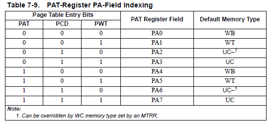
(This is from AMD64 Architecture Programmer's Manual Volume 2 System Programming 7.8.2 PAT Indexing, https://developer.amd.com/wordpress/media/2012/10/24593_APM_v21.pdf):
• PAT (page attribute table)—The PAT bit is bit 7 in 4-Kbyte PTEs; it is bit 12 in 2-Mbyte and 4-Mbyte PDEs.
Page-table entries that don’t have a PAT bit (PML4 entries, for example) assume PAT = 0.
• PCD (page cache disable)—The PCD bit is bit 4 in all page-table entries.
• PWT (page writethrough)—The PWT bit is bit 3 in all page-table entries.
As shown the dmesg log, the default PAT bit is 0, PCD bit is 1, PWT bit is 0. So PCD should be cleared to enable cache.
After our kernel code clear PCD flag, the PTE is properly changed as shown the dmesg (PAT, PCD, PWT = 0, 0, 0).
As shown Table 7-9, our PTE/PAT setting is WB (Write-Back) cache.
When I get response from AMD, I'll post it.
Thank you.
- Mark as New
- Bookmark
- Subscribe
- Mute
- Subscribe to RSS Feed
- Permalink
- Report Inappropriate Content
WOW, gyeong9m! Thanks much for the time you spent explaining all this. I will spend some time and see if I can understand it. Enjoy, John.
- Mark as New
- Bookmark
- Subscribe
- Mute
- Subscribe to RSS Feed
- Permalink
- Report Inappropriate Content
gyeong9m, there are lots I do not understand but I want to know what count=0 means in the MTRR? I found this:
* Releases an MTRR region. If the usage count drops to zero the
* register is freed and the region returns to default state."
Perhaps a problem? Enjoy, John.
- Mark as New
- Bookmark
- Subscribe
- Mute
- Subscribe to RSS Feed
- Permalink
- Report Inappropriate Content
Hi gyeong9m,
We are also trying to enable write-back for KC705 PCIe.
I was wondering if you have successfully enabled it? We tried some Intel CPU, but all freeze when enabling write-back.
You said it works like a write-through cache, so according to my understanding, read is successfully cached while write is not? Is that true?
Thank you very much.
Yu

