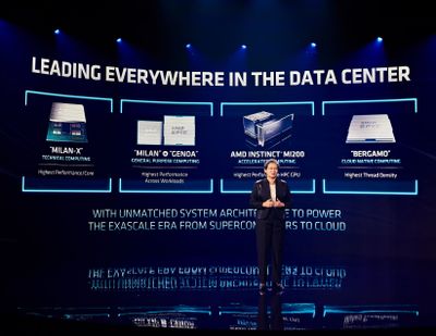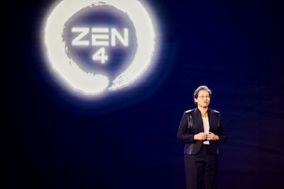
With larger remote workforces, the explosion of media streaming, and increasing impetus to reach scientific insights faster, businesses and organizations are looking for solutions that keep pace with their expanding data center needs. On November 8, Dr. Lisa Su unveiled multiple data center innovations from AMD -- new technology for technical computing, exascale-class accelerators, and a sneak peek at “Zen 4” data center products.
Meet “Milan-X”
At Computex in June, we previewed new 3D chiplet technology. Now, we are introducing the world to the 3rd Gen AMD EPYC™ processor with AMD 3D V-Cache technology, formerly code named “Milan-X.” Shipping in production volumes today, it is the first ever x86 CPU with true 3D die stacking. This stacking allows for 3 times the L3 cache compared to standard 3rd Gen AMD EPYC processors, relieving memory-bandwidth pressure and driving leadership performance. What does this mean for product design, one of the most compute intensive workloads?
- Accelerated simulation runs so design teams can solve problems faster, shorten design cycles, and get to market earlier
- More jobs and design iterations in the same amount of time, leading to higher quality and more innovative products
We are also collaborating with leading ISV and OEMs to develop turnkey solutions for customers. Since 3rd Gen AMD EPYC™ processor with AMD 3D V-Cache is fully compatible with existing “Milan” processors, it can be a drop-in replacement for their platforms. Solutions based on 3rd Gen AMD EPYC™ processor with AMD 3D V-Cache are slated to be available to customers starting in Q1 2022.
THE EXASCALE ERA BEGINS
Scientists and researchers are currently facing some of the biggest challenges and opportunities in human history. Enabling faster drug discovery for the treatment of diseases, weather modeling to understand and prepare for climate change, and exploring more efficient fuels and energy sources all require analyzing mind-boggling amounts of data, faster than ever before.
Our powerful new contribution toward these global imperatives? The new AMD Instinct™ MI200 series accelerators, the world’s fastest for HPC and AI.(1) With a dramatic 4X boost in performance for HPC applications over competitive GPUs, the MI200 will help computational researchers solve the world’s most challenging problems.(2)
The MI200, together with 3rd Gen AMD EPYC™ CPUs, will also power Oak Ridge National Laboratory’s Frontier supercomputer. Frontier will be capable of exascale computing—that means executing a billion computations per second! The exascale era is here, and AMD is leading the charge.
THE NEXT GENERATION
AMD is committed to driving even more innovation as we execute on our roadmap to raise the bar even higher for the data center. To that end, we unveiled the plans for the next generation of the EPYC processor line, based on our “Zen 4” microarchitecture, code named “Genoa” and “Bergamo.” “Genoa,” the flagship 4th Gen AMD EPYC processor, is designed to be the world’s highest performance processor for general purpose computing when it comes out next year. “Bergamo” is a purpose-built CPU specifically for cloud native computing, optimizing cache cores and power to deliver what cloud native applications demand. It is also socket compatible with “Genoa,” so it can be deployed on the same platforms already being qualified.

THIS IS ONLY THE BEGINNING
AMD isn’t taking our foot off the gas pedal. We will continue to drive data center modernization with innovative solutions that address the full spectrum of customer workloads through tailored approaches.
Did you miss the keynote? Watch it on demand.
ENDNOTES
1. World’s fastest data center GPU is the AMD Instinct™ MI250X. Calculations conducted by AMD Performance Labs as of Sep 15, 2021, for the AMD Instinct™ MI250X (128GB HBM2e OAM module) accelerator at 1,700 MHz peak boost engine clock resulted in 95.7 TFLOPS peak theoretical double precision (FP64 Matrix), 47.9 TFLOPS peak theoretical double precision (FP64), 95.7 TFLOPS peak theoretical single precision matrix (FP32 Matrix), 47.9 TFLOPS peak theoretical single precision (FP32), 383.0 TFLOPS peak theoretical half precision (FP16), and 383.0 TFLOPS peak theoretical Bfloat16 format precision (BF16) floating-point performance. Calculations conducted by AMD Performance Labs as of Sep 18, 2020 for the AMD Instinct™ MI100 (32GB HBM2 PCIe® card) accelerator at 1,502 MHz peak boost engine clock resulted in 11.54 TFLOPS peak theoretical double precision (FP64), 46.1 TFLOPS peak theoretical single precision matrix (FP32), 23.1 TFLOPS peak theoretical single precision (FP32), 184.6 TFLOPS peak theoretical half precision (FP16) floating-point performance. Published results on the NVidia Ampere A100 (80GB) GPU accelerator, boost engine clock of 1410 MHz, resulted in 19.5 TFLOPS peak double precision tensor cores (FP64 Tensor Core), 9.7 TFLOPS peak double precision (FP64). 19.5 TFLOPS peak single precision (FP32), 78 TFLOPS peak half precision (FP16), 312 TFLOPS peak half precision (FP16 Tensor Flow), 39 TFLOPS peak Bfloat 16 (BF16), 312 TFLOPS peak Bfloat16 format precision (BF16 Tensor Flow), theoretical floating-point performance. The TF32 data format is not IEEE compliant and not included in this comparison. https://www.nvidia.com/content/dam/en-zz/Solutions/Data-Center/nvidia-ampere-architecture-whitepaper..., page 15, Table 1. MI200-01
2. Calculations conducted by AMD Performance Labs as of Sep 15, 2021, for the AMD Instinct™ MI250 (128GB HBM2e OAM module) accelerator at 1,700 MHz peak boost engine clock resulted in 45.3 TFLOPS peak double precision (FP64) theoretical, floating-point performance. Calculations performed by AMD Performance Labs as of Sep 18, 2020 for the AMD Instinct™ MI100 accelerator designed with AMD CDNA 7nm FinFET process technology with at 1,502 MHz peak boost engine clock resulted in 11.535 TFLOPS peak theoretical double precision (FP64) floating-point performance. Published results on the NVidia Ampere A100 (80GB) GPU accelerator resulted in 9.7 TFLOPS peak double precision (FP64) theoretical, floating-point performance. Results found at:https://www.nvidia.com/content/dam/en-zz/Solutions/Data-Center/nvidia-ampere-architecture-whitepaper... MI200-08